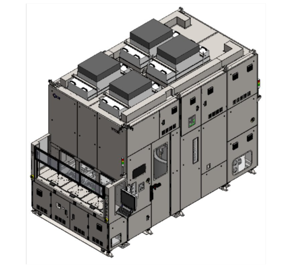
World's First Dual Chamber FOUP Cleaning System
Industry-leading FOUP cleaning system with separate chambers for Body and Cover cleaning - a world-first innovation. Features the smallest floor area in its class (2,140 x 3,290 x 3,160 mm), with throughput of 20 FOUP/hr for both NFC300 (Non Vacuum) and VFC301 (Vacuum) models. Equipped with advanced N2 Purge and FOUP Leak Check System at loader/unloader, achieving exceptional cleaning quality with minimal ion, metal, and organic contamination.
Advanced Processing
Specialized cleaning and drying technology for 300mm wafer containers, ensuring optimal semiconductor manufacturing conditions
Precision Control
Advanced automation and environmental control systems for consistent and reliable wafer container processing
Key Features
Experience the cutting-edge features that make our FOUP/FOSB Cleaning System the industry's most advanced solution.
Superior Dual Chamber Design
World's first separate cleaning chambers for FOUP Body and Cover, delivering better cleaning power and improved throughput with reduced cleaning time.
Compact & Efficient Design
Industry's smallest footprint with dimensions of 2,140 x 3,290 x 3,160 mm, maintaining high throughput of 20 FOUP/hr for both vacuum and non-vacuum models.
Advanced Quality Control
Integrated N2 Purge and FOUP Leak Check System at loader/unloader, with exceptional error rate of 0.31/large/month. Currently used by leading Silicon Ingot Companies.
Curator's Comments
"The Dual Chamber FOUP/FOSB Cleaning System represents a breakthrough in semiconductor manufacturing technology. Its innovative separate chamber design for body and cover cleaning, combined with the industry's smallest footprint, sets new standards for efficiency and contamination control in wafer handling."
Where precision meets innovation—advancing semiconductor manufacturing excellence.
Market Insight
The dual chamber system revolutionizes FOUP cleaning with its innovative design, addressing the critical need for ultra-clean wafer containers in advanced semiconductor manufacturing. The exceptional error rate of 0.31/large/month demonstrates its reliability in maintaining the highest cleanliness standards.
Process Innovation
Advanced cleaning technology meets semiconductor grade requirements
Ready to Transform Your Factory?
Contact our team to schedule a demo or discuss your specific requirements.
Contact Information
Address
1629 K St NW Suite 800
Washington 20006, United States
Phone
(920) 671-1632
info@koreaninnovation.com